



Semiconductor Gas Sensors
Semiconductor gas sensors—often called MOS or MOX sensors—detect gases through surface reactions on a heated metal-oxide sensing layer. Those reactions change charge-carrier density and therefore sensor resistance. The technology is compact, sensitive and versatile, but it is also broadband-sensitive, temperature-dependent and strongly influenced by calibration, heater conditions and the surrounding gas matrix.
In clean air, oxygen adsorbs on the heated metal-oxide surface and captures electrons. The electron-depletion layer is relatively large, so a typical n-type SnO₂ sensor shows higher resistance.
*Vout direction assumes a common divider with Rs above RL. Values are illustrative, not calibration data.
Working principle
How does a semiconductor gas sensor work?
The MOS measurement chain
- Heater: raises the sensing material into a useful reaction-temperature window.
- Metal-oxide surface: SnO₂ and other metal oxides provide the active gas-sensitive surface.
- Adsorbed oxygen: captures electrons and helps create a surface depletion region in typical n-type material.
- Target-gas reaction: reducing or oxidizing species shift the surface charge balance.
- Resistance change: the sensor electronics measure the resulting change in Rs.
A useful classical explanation is Figaro’s MOS operating-principle guide, which describes heated SnO₂, oxygen adsorption and electron release during reducing-gas exposure: Figaro MOS operating principle ↗.

Sensor construction
What is inside a semiconductor gas sensor?

A semiconductor element is not simply a piece of “gas-sensitive material.” Its mechanical package, heater, substrate and electrodes define how the sensing layer is heated, exposed to gas and electrically measured.
Protective mesh / cap
Allows diffusion while helping protect the hot sensing structure from particles, contact and mechanical damage.
Sensing layer
Metal oxide, catalyst additives and microstructure determine sensitivity, cross-response and useful operating temperature.
Electrodes + substrate
Provide electrical contact and high-temperature support for the gas-sensitive film.
Heater
Controls the surface chemistry. Traditional ceramic heaters and MEMS micro-hotplates differ greatly in thermal mass and power.
Surface chemistry
Why reducing gases often decrease resistance while oxidizing gases increase it
For a typical n-type MOS material such as SnO₂, the surface depletion layer is the key. Reducing gases tend to return electrons to the material; oxidizing gases tend to withdraw more electrons.

Reducing gases
- Examples: CH₄, CO, H₂, many VOCs
- React with or consume adsorbed oxygen
- Release electrons back into n-type material
- Depletion layer narrows
- Rs usually decreases
Oxidizing gases
- Examples: NO₂, O₃
- Can withdraw additional electrons from the surface
- Electron depletion increases
- Depletion layer widens
- Rs usually increases
Thermal control
Why does a semiconductor gas sensor need a heater?
The heater is one of the most important parts of a MOS sensor. It puts the sensing layer in a temperature region where oxygen adsorption, desorption and target-gas reaction rates are useful and repeatable.
- Surface activation: many useful MOS reactions are too slow at room temperature.
- Sensitivity tuning: different gases can peak at different operating temperatures.
- Response and recovery: temperature affects both reaction speed and desorption.
- Power trade-off: traditional heaters can consume hundreds of milliwatts, while MEMS hotplates can reduce thermal mass dramatically.
A heater setpoint is not universal. The best temperature depends on the metal oxide, catalyst, package, target gas, expected interference and the chosen measurement algorithm.

Electrical readout
Rs, R0, RL and Vout: what a raw MOS sensor actually outputs

Basic divider
Vout = Vc × RL / (Rs + RL)
- Rs: sensor resistance under the current gas condition.
- R0: a baseline or reference resistance defined under specified reference conditions.
- RL: load resistor used to convert resistance change into voltage.
- Vout: measured divider voltage; with Rs above RL, Rs down usually means Vout up.
- Rs/R0: a commonly used normalized response ratio for sensitivity curves.
Why ppm conversion is not one equation
Concentration estimation normally depends on the sensor-specific sensitivity curve plus the reference condition, heater condition, temperature, humidity, gas composition and calibration method. A raw ADC count should not be treated as a universal ppm value.
Technology evolution
Traditional MOS vs MEMS MOX
The sensing chemistry can be similar while the thermal architecture changes radically. A MEMS micro-hotplate uses very low thermal mass, enabling lower heater power, faster temperature transitions and more advanced heater cycling.
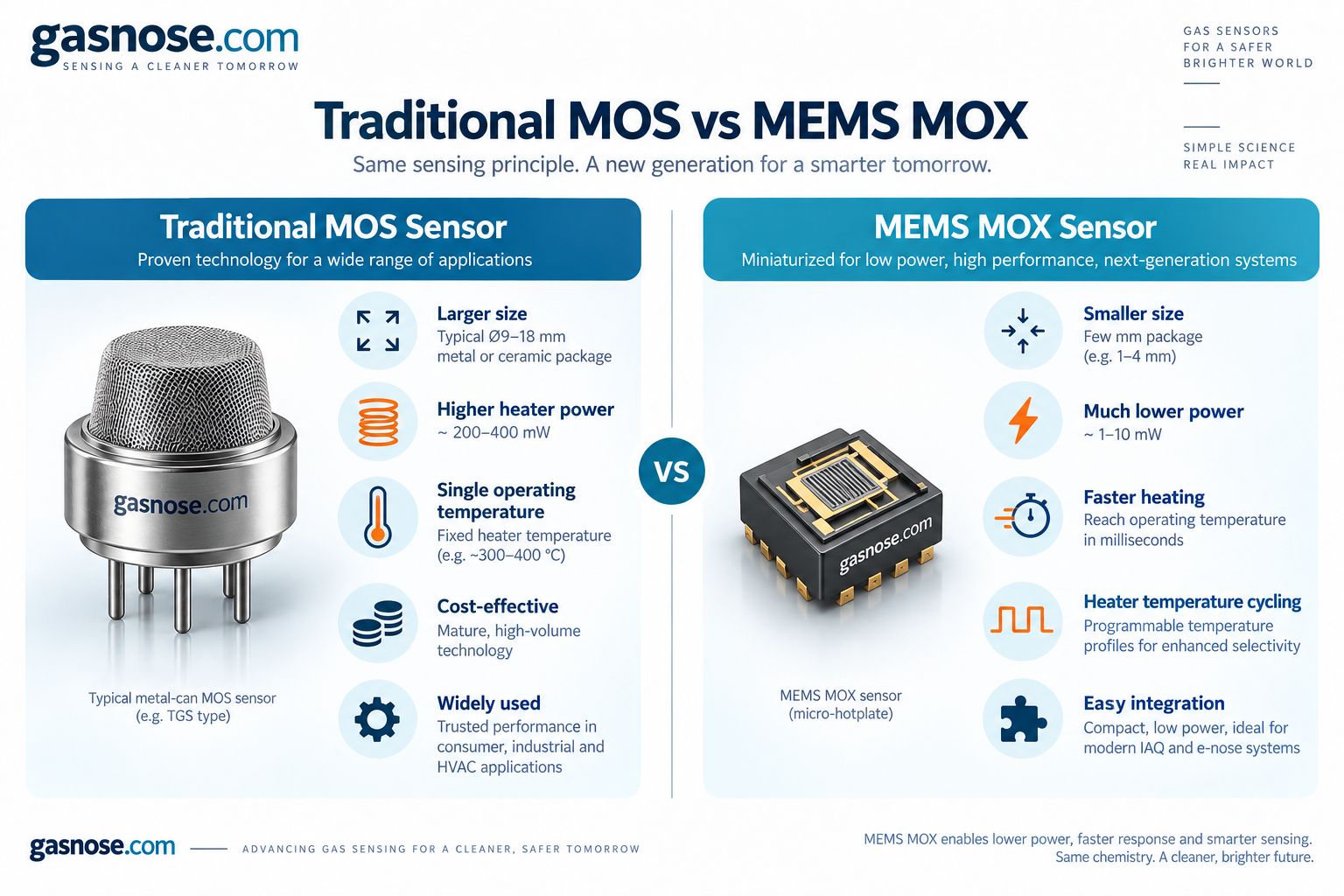
| Design factor | Traditional MOS | MEMS MOX |
|---|---|---|
| Heater | Ceramic or planar heater with larger thermal mass | Micro-hotplate fabricated on a silicon/MEMS structure |
| Power | Often tens to hundreds of mW depending on product | Can be substantially lower because the heated mass is small |
| Temperature control | Often one fixed or slowly switched condition | Fast temperature cycling and heater profiles are practical |
| Package | Metal-can, ceramic or through-hole formats are common | Compact ceramic/SMD packages are common |
| Algorithm potential | Excellent for conventional alarm and trend sensing | Well suited to multi-temperature fingerprints and electronic-nose approaches |
Technology fit
Which gases are best suited to semiconductor sensors?

Broad practical use
CH₄ / natural gas, LPG / propane / butane, H₂, alcohol / ethanol, VOC / odor and combustion-related gases are classic MOS application families.
Needs tailored design
CO, NH₃, H₂S, NO₂, O₃, formaldehyde and refrigerants can be detected with suitable MOS materials and calibration.
When selectivity matters most
CO₂ commonly favors NDIR/PAS; O₂ favors electrochemical or paramagnetic methods; highly compound-specific VOC work may favor PID or analytical methods.
Engineering trade-offs
Semiconductor gas sensor advantages and limitations
Why engineers choose MOS
- High sensitivity with relatively simple electrical readout
- Broad gas coverage across combustible, VOC and pollution applications
- Compact sensor elements and mature manufacturing
- Fast response possible with appropriate heater and diffusion design
- MEMS versions can offer very small packages and low heater power
- Temperature cycling and sensor arrays can create rich response fingerprints
Where MOS needs engineering care
- Cross-sensitivity to other reducing or oxidizing gases
- Strong temperature and humidity influence
- Warm-up, baseline stabilization and long-term drift
- Heater power and thermal interaction with the enclosure
- Poisoning, siloxane contamination and VOC overload
- Raw resistance does not automatically equal a selective ppm measurement
Selectivity and environment
Why MOS sensors are cross-sensitive—and why temperature and humidity matter
MOX sensors are often intentionally broad-band sensitive. That makes them useful for air quality, odor, leak detection and classification, but it also means multiple gases can produce overlapping response patterns.
- Gas overlap: ethanol, acetone, methane and other VOCs can all shift the same sensor resistance.
- Humidity: water vapor competes for surface sites and changes adsorption chemistry and baseline.
- Temperature: both the environment and heater operating point alter reaction kinetics and sensitivity.
- Compensation: application-ready modules often combine temperature/RH sensing, calibration and algorithms.
A digital output labelled “VOC” or “NOx index” should be understood as an interpreted sensor signal—not proof that the underlying MOX element has become chemically selective to one molecule.
Sensirion describes the SGP41 as a digital MOX sensor with VOC/NOx signals, humidity compensation and broad sensitivity to typical VOCs: Sensirion SGP41 ↗.

Baseline stability
Warm-up, aging and drift: why a MOS sensor may not be ready immediately after power-on
Warm-up
The heater and sensing surface need time to reach a stable thermal and adsorption state after power is applied.
Burn-in / aging
Manufacturers may age elements to improve repeatability before calibration or module assembly.
Baseline drift
Long-term surface changes, contamination and operating history can gradually move the clean-air or reference resistance.
Storage history
Moisture, packaging, inactive storage and first power-on after shipment can change how quickly a stable baseline returns.
Contamination risk
What can poison or contaminate a semiconductor gas sensor?
Because the sensing mechanism occurs at the surface, materials that block, react with or permanently modify active sites can change sensitivity and baseline.
- Siloxanes: common in personal-care products, adhesives and some sealants; they can create persistent surface contamination.
- High VOC exposure: overload or prolonged exposure can shift baseline and recovery behavior.
- Sulfur compounds: can interact strongly with catalysts and metal-oxide surfaces.
- Dust, oil and aerosols: may block diffusion or coat the sensing surface.
- Cleaning chemicals: solvents and vapors around manufacturing or maintenance areas can become strong interferents.
Design countermeasures
- Choose enclosure vents, membranes and filters for the actual contamination environment.
- Keep silicones, adhesives and conformal coatings away from the sensing airflow unless validated.
- Define high-concentration exposure and recovery tests.
- Use diagnostics or baseline tracking when the application requires long unattended life.
- Validate the complete product—not only the bare element—against the expected contaminants.
Advanced MEMS sensing
Heater temperature cycling, gas fingerprints and AI
One heater, multiple reaction windows
A MEMS hotplate can move rapidly between temperature steps. The same gas mixture may produce a different resistance pattern at each step, creating a richer fingerprint than a single fixed-temperature reading.
Why temperature profiles help
- Different surface reactions dominate at different temperatures.
- Rapid MEMS heating makes multi-step profiles practical.
- Feature extraction can use peak response, slope, recovery and cross-channel patterns.
- Machine-learning models can classify known conditions when training data represents the real application.
This is the bridge from a conventional MOS element to a modern electronic-nose architecture.
Applications
Where semiconductor gas sensors are commonly used
Gas leak alarms
Methane, LPG, hydrogen and other combustible-gas detection in residential, commercial and industrial products.
Indoor air quality
VOC, odor, smoke and pollution trend sensing in air purifiers, ventilation equipment and smart-home devices.
Automotive
Cabin air-quality control, odor classification and external pollution monitoring with compact MEMS arrays.
Industrial safety
Application-specific detection of combustible and selected toxic gases where the MOS cross-response is acceptable or compensated.
Refrigeration and HVAC
Refrigerant leak detection and IAQ monitoring with gas-specific semiconductor materials and modules.
Electronic nose
Multi-sensor or multi-temperature pattern recognition for odor, process, appliance and intelligent classification tasks.
Integration level
Sensor element vs sensor module
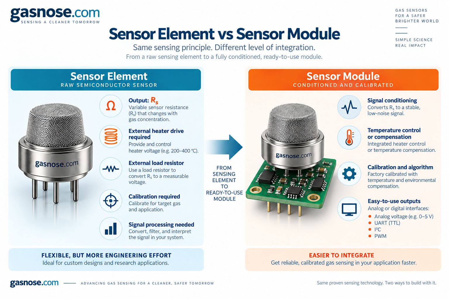
The raw element is only the sensing transducer. The closer a product moves toward a calibrated module, the more heater control, analog front end, compensation, calibration and algorithms shift from the OEM into the sensing product.
Raw element
Rs output, external heater drive, RL selection, ADC design, calibration and algorithm work remain with the OEM.
Conditioned module
Signal conditioning, temperature compensation, factory calibration and analog/digital interfaces simplify integration.
For OEM design, this choice often matters more than whether the sensing chemistry is described simply as “semiconductor.”
Technology benchmarks
How modern MOS platforms are implemented
These examples illustrate different implementation directions rather than forming a ranking.
| Platform | What it represents | Engineering lesson |
|---|---|---|
| Figaro TGS / MOS family | Classic heated SnO₂ semiconductor sensing | A clear reference for oxygen adsorption, reducing-gas reaction and resistance-based readout. |
| Sensirion SGP41 | Digital MOX with VOC and NOx outputs | Modern MOX can combine micro-hotplates, humidity compensation and application-oriented gas-index algorithms. |
| Bosch BME688 class | MEMS gas sensing with programmable heater profiles | Temperature profiles can generate multidimensional gas-response features for classification. |
| SGX4410 / SGX6410 class | MEMS metal oxide + embedded processing | Compact platforms increasingly combine MOX hardware with compensation and machine-learning-based outputs. |
For examples of current digital MOX and AI-assisted implementations, see Sensirion SGP41 ↗ and SGX4410 ↗.
Example OEM implementations
Representative semiconductor sensor products
These examples show how the same MOS concept evolves from traditional planar sensing to MEMS elements, conditioned modules and multi-channel electronic noses.
| Example | Type / target | What it demonstrates | Integration note |
|---|---|---|---|
| Winsen MP-4 | Traditional planar MOS / methane | Classic heater + metal-oxide element; heater consumption ≤350 mW | Raw resistance output; OEM drive and calibration required |
| Winsen MP503 | Traditional air-quality MOS / alcohol, smoke, VOC-related gases | Broad air-quality response using a planar semiconductor structure | Useful for trend / control applications after calibration |
| Winsen GM-402B | MEMS combustible MOX / CH₄, C₃H₈ | 5 × 5 × 1.55 mm MEMS package, heater consumption ≤80 mW | Compact low-power combustible sensing |
| Winsen GM-502B | MEMS VOC MOX | 5 × 5 × 1.55 mm MEMS package, heater consumption ≤50 mW | VOC / IAQ-oriented raw MEMS element |
| Winsen GM-102B | MEMS NO₂ MOX | Example of an oxidizing-gas semiconductor route | Shows that MOX is not limited to reducing gases |
| Winsen ZP01-MP503 | Conditioned air-quality module | Raw MOS element integrated with aging, calibration, self-check and TTL output | Lower OEM analog/calibration burden |
| Winsen ZM101-A AI-Nose | Six-channel MEMS gas sensor array | Multi-channel response, T/RH compensation and AI-model integration | Electronic-nose classification platform |
Selection workflow
How to choose a semiconductor gas sensor
1. Define the sensing job
Alarm, trend, control, classification and quantitative ppm measurement are different requirements.
2. Define the gas matrix
List the target gas, likely interferents, oxygen availability, humidity and background VOCs.
3. Define the environment
Temperature, RH, contamination, airflow, enclosure materials and warm-up duty can dominate field performance.
4. Define integration level
Choose raw element, conditioned module or smart array based on analog design skill, calibration resources and time-to-market.
Before design freeze
- Target concentration range and alarm points
- Required selectivity versus expected interferents
- Fixed heater or heater cycling
- Power budget and thermal constraints
- Warm-up and duty-cycle behavior
- Calibration / baseline strategy
- Temperature and humidity compensation
- Lifetime, contamination and recovery tests
Engineering checklist
For OEM selection, record the full application—not just the gas name.
- Target gas and other gases present
- Alarm / trend / ppm / classification goal
- Ambient temperature and RH envelope
- Expected siloxanes, aerosols and cleaning chemicals
- Enclosure airflow and diffusion path
- Power-on / standby / cycling strategy
- Analog, UART, I²C or other interface
- Production calibration and field verification plan
Useful Gas Nose tools: Gas Sensor Product Finder and Gas Concentration Converter.
FAQ
Semiconductor gas sensor FAQ
What is a semiconductor gas sensor?
A semiconductor gas sensor uses a gas-sensitive semiconductor—commonly a heated metal oxide—to convert surface gas reactions into a change in electrical resistance or conductivity.
How does a MOS gas sensor work?
In a typical n-type MOS sensor, oxygen adsorbs on the heated surface and captures electrons. Reducing or oxidizing gases then change the surface oxygen and charge state, which changes the depletion layer and sensor resistance.
Why does a semiconductor gas sensor need a heater?
The heater activates surface chemistry, stabilizes oxygen adsorption and controls reaction, response and recovery rates. The optimum heater condition depends on material and target gas.
What are Rs and R0?
Rs is the sensor resistance under the current measurement condition. R0 is a reference or baseline resistance defined under specified conditions. Many MOS datasheets use the normalized ratio Rs/R0 or R0/Rs to describe sensitivity.
Why do reducing gases decrease resistance in many MOS sensors?
In a typical n-type material such as SnO₂, reducing gases consume adsorbed oxygen and release electrons back into the semiconductor, narrowing the depletion region and usually decreasing resistance.
What is the difference between traditional MOS and MEMS MOX?
The surface chemistry can be similar, but MEMS MOX uses a micro-hotplate with much smaller thermal mass. This enables lower heater power, faster temperature transitions, compact packaging and programmable heater profiles.
Which gases are best detected by MOS sensors?
MOS is commonly used for methane, LPG, hydrogen, alcohol, VOCs, odor and smoke, and application-specific designs can also target CO, NH₃, H₂S, NO₂, O₃, formaldehyde and some refrigerants.
Why are MOS sensors cross-sensitive?
The sensing surface can react with many reducing or oxidizing species. Different gases may produce overlapping resistance responses, so material selection, filters, heater control, compensation and algorithms are used to improve application-level discrimination.
How do temperature and humidity affect MOS sensors?
They change adsorption, reaction kinetics and baseline resistance. Water vapor can occupy surface sites and ambient temperature changes both the gas chemistry and thermal operating conditions, so compensation and validation are often required.
Can a MOS sensor measure exact ppm?
It can be calibrated for quantitative measurement in suitable applications, but a raw MOS element does not inherently output ppm. Accurate concentration estimation requires a sensor-specific calibration model and control of heater, environment, interferents and reference conditions.
Can AI make a MOS sensor gas-specific?
AI can classify patterns across temperature, time or multiple sensor channels, but it does not make the underlying metal-oxide surface perfectly molecule-specific. Model performance depends on representative training data and the real application gas matrix.
Need to choose a semiconductor sensing architecture?
Start with the target gas and the actual measurement goal, then define cross-sensitivity, heater power, temperature/RH range, contamination risk, calibration resources and integration level. The right MOS solution is usually the one matched to the real gas matrix—not simply the sensor with the highest nominal sensitivity.